
| About MicroField
|
Technical meeting on April 23rd
14 May 2020
by Super User
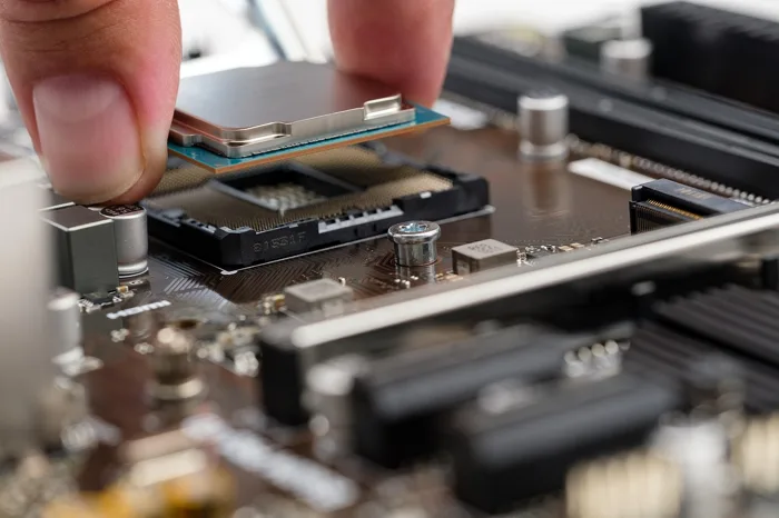
The MicroField team convened on 23rd April 2020 for a productive technical meeting. Discussions focused on advancing the latest developments in microelectronics and semiconductor manufacturing processes. Key areas explored included innovative approaches to micro-transfer-printing and the integration of smart systems. The group also reviewed progress in chip design and testing methodologies.
MicroField at Photonics West
11 February 2020
by Super User
Photonics West, a significant industry event, recently concluded in San Francisco. The conference attracted an exceptionally large audience, exceeding 20,000 attendees, highlighting the sustained interest and growth within the photonics and related technology sectors. This gathering provided a vital platform for professionals to share the latest advancements and discuss future trends shaping the industry.
A special MicroField session will be held at the Waferbond Conference, focusing on cutting-edge advancements in semiconductor manufacturing. The discussions will delve into novel techniques for wafer bonding, a critical step in the fabrication of advanced microelectronic devices. Attendees can expect insights into next-generation interconnect technologies and their impact on system performance and miniaturisation.
03 January 2020
by Super User
The foundry recently contributed to a dedicated session on MicroField technologies at the International Conference on Wafer Bonding, held in late 2019. This event provided an excellent platform for discussing advancements in wafer bonding and its integration with microelectronics fabrication processes. The session fostered valuable exchanges and brought together leading experts in the field.
Workshop on µTP design support tools This workshop delves into the latest advancements in design support tools for micro-transfer printing (µTP) processes. We will explore innovative software solutions and methodologies that streamline the design and optimisation of µTP processes, fostering greater efficiency and precision in semiconductor manufacturing. Attendees will gain insights into how these tools can accelerate the development cycle for complex microelectronic systems. Discussions will cover key features and applications, enabling participants to leverage these resources effectively in their own research and development.
06 December 2019
by Super User
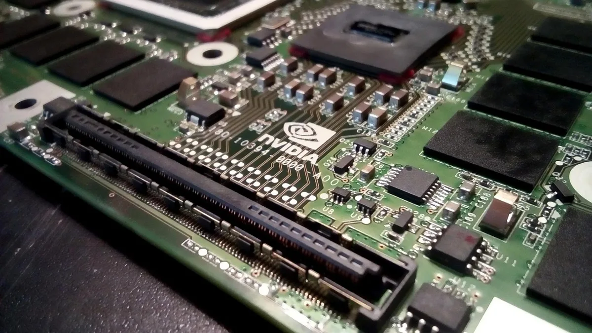
The collaborating organisations, comprising a research institution, a semiconductor foundry, and a technology development partner, convened for a joint workshop on 26th November. The primary focus was to thoroughly assess the present state of the µTP design support tool and to engage in a detailed discussion regarding potential enhancements and modifications. This collaborative session aimed to ensure the tool's continued effectiveness and alignment with evolving industry needs in microelectronics design.
Cu-RDL development
23 October 2019
by Super User
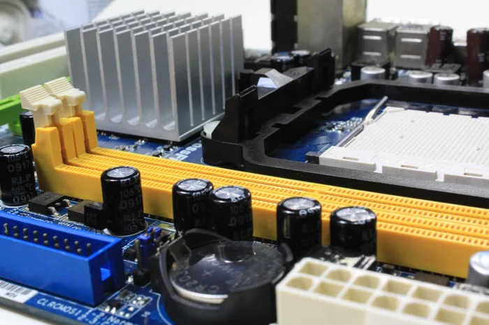
During the past month, our foundry has successfully processed a batch of wafers containing test chiplets. This work was focused on developing our copper Redistribution Layer (RDL) processing capabilities, utilising our state-of-the-art electroplating tool situated within our MEMS cleanroom. This advancement is a significant step towards enabling more complex and efficient semiconductor architectures.
The team convened for a crucial technical meeting. This gathering focused on advancing key research objectives within the semiconductor and microelectronics domain. Discussions covered innovative fabrication techniques, system-level integration strategies, and the rigorous testing methodologies essential for next-generation smart systems. Progress was reviewed across several work packages, setting the stage for future development and collaborative efforts.
05 April 2019
by Super User
In late 2019, the MicroField team convened for another productive technical meeting. Discussions focused on advancing key areas within microelectronics and semiconductor manufacturing, with a particular emphasis on innovative techniques like micro-transfer-printing for novel applications. The agenda also covered progress in smart-system integration and the intricate challenges of chip design and testing.
Smart Systems Integration (SSI) This event delves into the intricate world of smart systems integration, a critical area for the advancement of modern electronics. It provides a platform for discussing cutting-edge developments in semiconductor manufacturing and chip design, crucial for creating sophisticated, interconnected devices. Attendees can expect insights into novel microelectronics technologies and their application in a wide range of smart systems. The focus remains on fostering innovation and collaboration within the semiconductor technology landscape.
25 April 2019
by Super User

The foundry exhibited and presented at the Smart Systems Integration event. This significant industry gathering provided a platform to showcase advancements in semiconductor manufacturing and smart system integration. Discussions at the event centred on the latest developments in chip design, testing, and the practical application of microelectronics in complex systems.
Meeting to discuss a Design tool developed within the MicroField project. This discussion will focus on a novel design tool, a key outcome of the MicroField initiative. The tool aims to streamline and enhance the microelectronics design process, addressing current industry challenges. Attendees will explore its capabilities and potential applications in semiconductor manufacturing and smart-system integration.
26 March 2019
by Super User

In early 2019, a meeting was held to review a significant design tool that has been developed. This innovative tool is set to enhance our capabilities in microelectronics design and was discussed at the foundry. The session focused on its potential applications and future development within the semiconductor technology landscape.
Technical meeting
05 April 2019
by Super User
In the spring of 2019, members of the MicroField initiative convened for a productive technical meeting. This gathering provided an essential forum to discuss advancements and challenges in the field of microelectronics and semiconductor technology. Participants shared insights and explored new avenues for innovation, reinforcing the collaborative spirit driving the project.
Industry Electronics Forum 2019
26 November 2018
by Super User

This leading industry conference, held in late 2019, is a key event for professionals across the electronics sector. This annual gathering provides a crucial platform for discussing advancements and future directions in microelectronics and semiconductor technology. Attendees can expect insightful presentations and valuable networking opportunities within this dynamic field.
Third Technical Meeting
31 October 2018
by Super User
The MicroField team convened for a technical meeting in the autumn of 2018. This gathering provided an excellent opportunity for participants to discuss advancements in microelectronics and semiconductor technology. The event fostered collaborative progress on innovative solutions for smart system integration and chip design challenges.
First-year progress update
19 June 2018
by Super User
With the initial twelve months of work now complete, the project's collaborators convened to showcase their progress and preliminary findings to an audience of stakeholders and independent technical specialists. This milestone marked a crucial juncture for reviewing the advancements made in the field.
Second Technical Meeting
14 March 2018
by Super User
The MicroField team convened for a productive technical meeting in early 2018. Fortunately, the severe snowstorm experienced the previous week had subsided, allowing the event to proceed as scheduled. This meeting provided a valuable opportunity for participants to advance discussions on key aspects of microelectronics and semiconductor technology development.
The first technical meeting is set to take place soon. This gathering will serve as an important forum for discussions related to the latest advancements in microelectronics and semiconductor technologies. Attendees can expect to engage in insightful exchanges about innovative manufacturing processes, micro-transfer-printing techniques, and the integration of smart systems. This meeting promises to be a pivotal moment for professionals in the field to share knowledge and foster collaboration.
12 October 2017
by Super User
In late 2017, the inaugural MicroField Technical Meeting was held at a leading microelectronics research facility. This event gathered experts and enthusiasts from the microelectronics and semiconductor sectors to discuss advancements and innovations in the field. Attendees had the opportunity to share insights on cutting-edge technologies, fostering collaboration and knowledge exchange among professionals dedicated to pushing the boundaries of micro-transfer printing and smart system integration.
MicroField Launch Event - This event marks the beginning of a significant venture into the realms of microelectronics and semiconductor technology. Industry experts gathered to discuss the latest advancements and collaborative opportunities within micro-transfer printing techniques, smart-system integration, and cutting-edge chip design and testing methodologies. The insights shared during this gathering aim to pave the way for innovation and growth in the microelectronics sector, fostering a collaborative spirit among participants.
23 February 2017
by Super User
In the spring of 2017, the MicroField initiative commenced successfully, marking a significant milestone in the development of microelectronics and semiconductor technologies. This project aims to explore innovative approaches and methodologies in the field, paving the way for advancements in micro-transfer printing, smart system integration, and chip design and testing. The commencement of this initiative highlights a commitment to progressing the industry and fostering new solutions.
